|
LabGuy's World: 'Tiny Ike' - Iconoscope TV Camera Project
PART FOUR - DEFLECTION & BLANKING CIRCUITS. "We are the joy boys of video! We push electrons to and fro!" 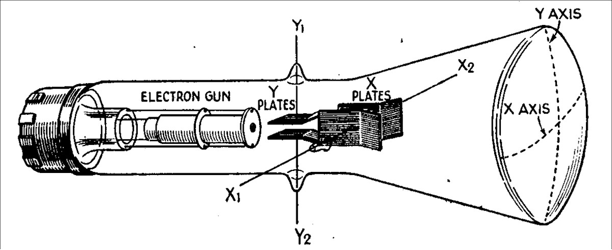
Electrostatic Deflection in Cathode Ray Tubes The 5527 iconoscope uses electrostatic deflection. No cumbersome and power hungry heat generating magnetic coils required. No sir! In electrostatic deflection, the electron beam is passed between two parallel metal plates. If both plates are the same voltage, the beam passes straight through. If there is a voltage difference between the plates, the beam will be attracted to the positive plate and repelled by the negative plate. The amount of beam deflection is proportional to the applied voltage between the plates. There are two pairs of plates, positioned at 90 degrees to each other. One set for vertical deflection (Y). The other set for horizontal (X). This is the mechanism that "samples" the image projected onto the mosaic plate by the lens at the front of the camera tube. In the 5527, the vertical deflection plates are called DJ1 & DJ2. The horizontal plates are DJ3 & DJ4. 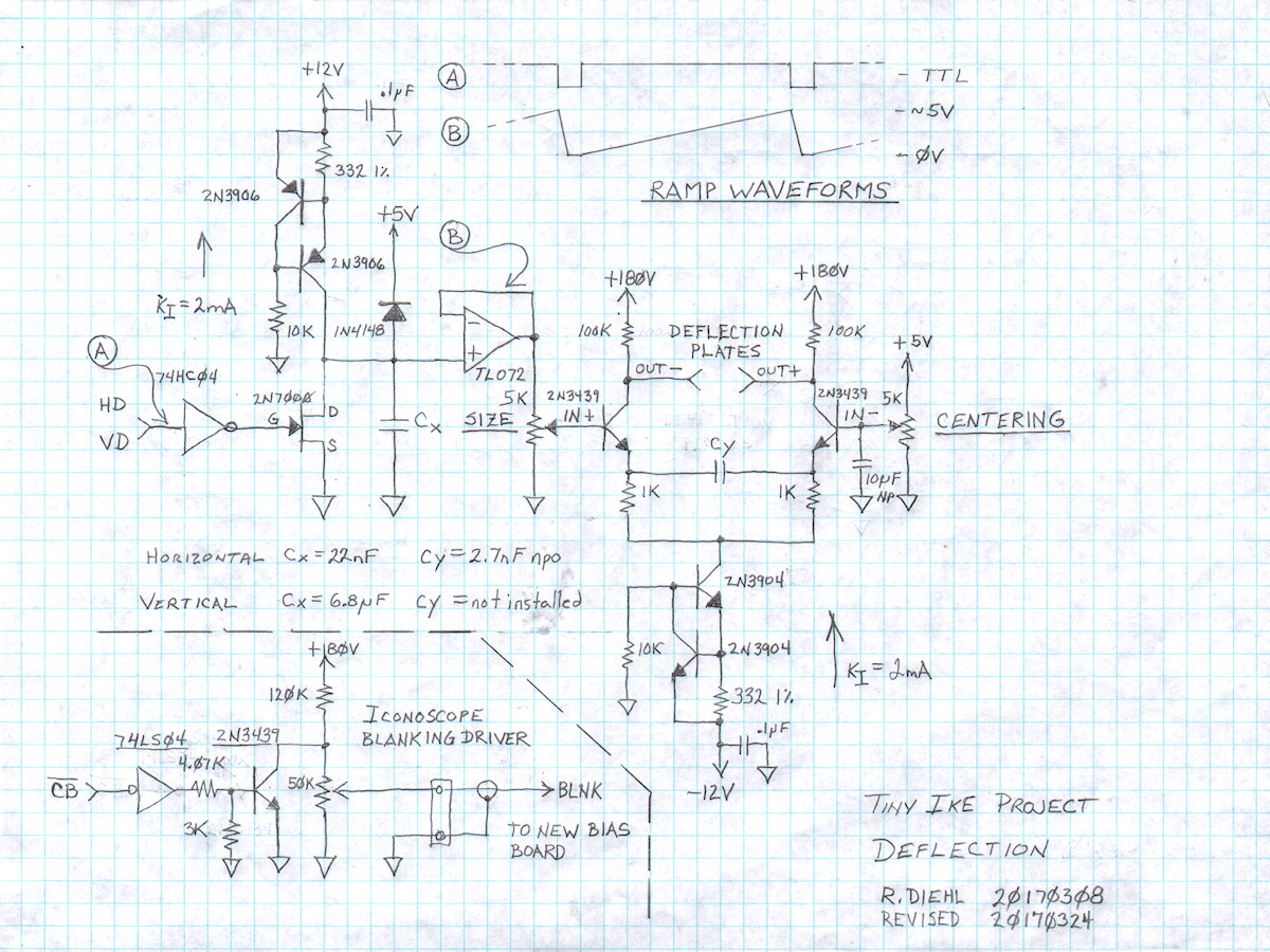
Blanking & Deflection Schematic - Revised: 20170324 (Original Schematic) Blanking is the process of turning the electron beam off and on at the right times during the scan. This prevents the retracng beam from partially discharging the mosaic and making visible retrace lines in the video. The blanking amplifier is in the lower left corner of the schematic above. It boosts five volt composite blanking not (CB) from the sync generator to about 30 volts to cut off the beam in the 5527. When composite blanking (CB) is low, the transistor turns on and zero volts is output. When composite blanking (CB) is high the transistor turns off and about 50 volts appears at the top of the 50K pot, a simple level control. This HV blanking pulse is sent via coax to the new bias board where it is AC coupled to the control grid. The amplitude of the output pulse can be adjusted (scaled) since I don't know the exact voltage required at the time of the initial design. Ramp Generator CircuitSync generator pulses, horizontal drive (HD) or vertical drive (VD), are inverted to drive a FET switch (2N7000) that is wired in parallel with a capacitor. This capacitor (Cx) is charged by the 2mA constant current source composed of two PNP transistors (2N3906). When the drive pulse goes low, the FET (2N7000) is switched on and shorts out the charge in the capacitor, resetting it to zero volts. When the drive pulses returns to a high, during active scanning, the capacitor charges in a linear ramp until it reaches 5.6 volts, and is clamped by the diode (1N4148), or the next drive pulse arrives. The capacitor value is the only difference between the horizontal and vertical scan circuits. For horizontal scan, the capacitor (Cx) is 22nF (.022uF) and for vertical scan, 6.8uF. The ramp voltage is buffered by an opamp and passed on to the high voltage differential amplifier by way of the size control. Deflection Amplifer CircuitThe deflection amplifiers use two 2N3439 high voltage transistors operating at 180 volts. These are configured into two classic differential amplifiers with a gain of approximatel 100. The gain is actually 200 if you factor in the differential effect. This is far more gain than required for the 5527. The scan size control adjusts the amplitude of drive applied to the amplifier and the centering control sets the average DC of both collectors to the same voltage. The differential output, from the collectors, is sent directly to the iconoscope deflection plates. 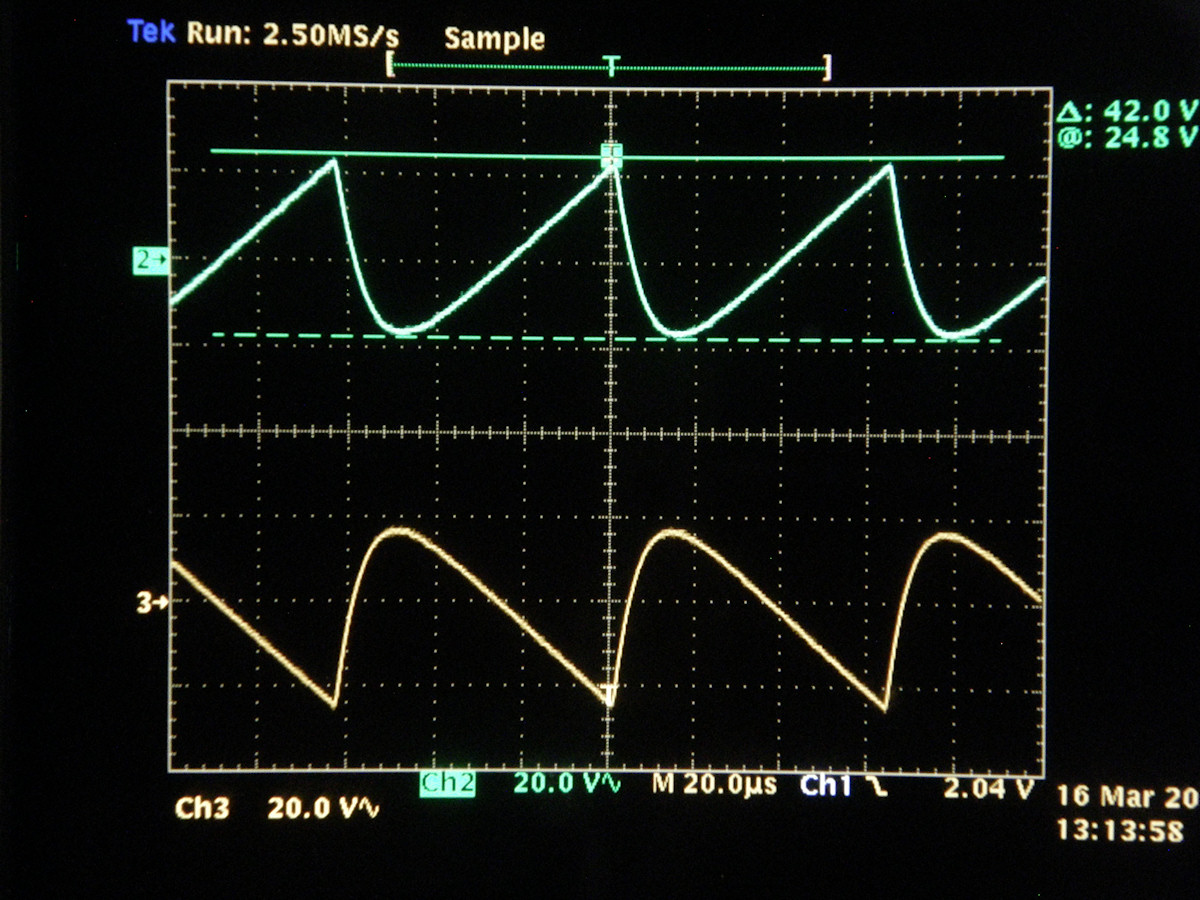
Horizontal Deflection with Poor Frequency Response - 20170316 These deflection amplifiers don't have a very high bandwidth. Rolloff begins around three or four kilohertz. For the vertical scan running at 60 Hertz, this is more than sufficient bandwidth to reproduce very good output waveforms. The horizontal scan, at 15,734 Hertz shows significant rolloff without compensation. To fix the rolloff, a capacitor (Cy) is placed between the emmitters of the 2N3439 output transistors. As frequency increases, Cy will begin to decrease the apparent value of the 1K resistors by acting as an AC shunt. As this apparent resistance decreases, the gain of the amplifier increases. The value of the capacitor was chosen emperically by trying different values until an optimum waveshape was achieved. The optimally discovered value for Cy was 2.7nF (2700pF). 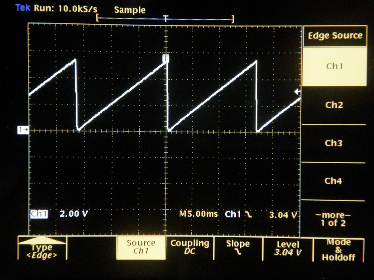
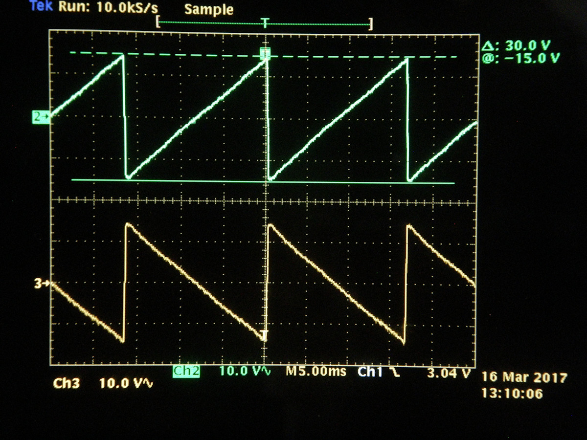
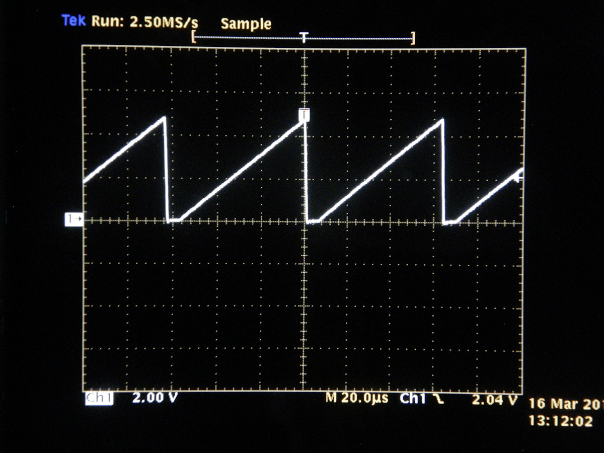
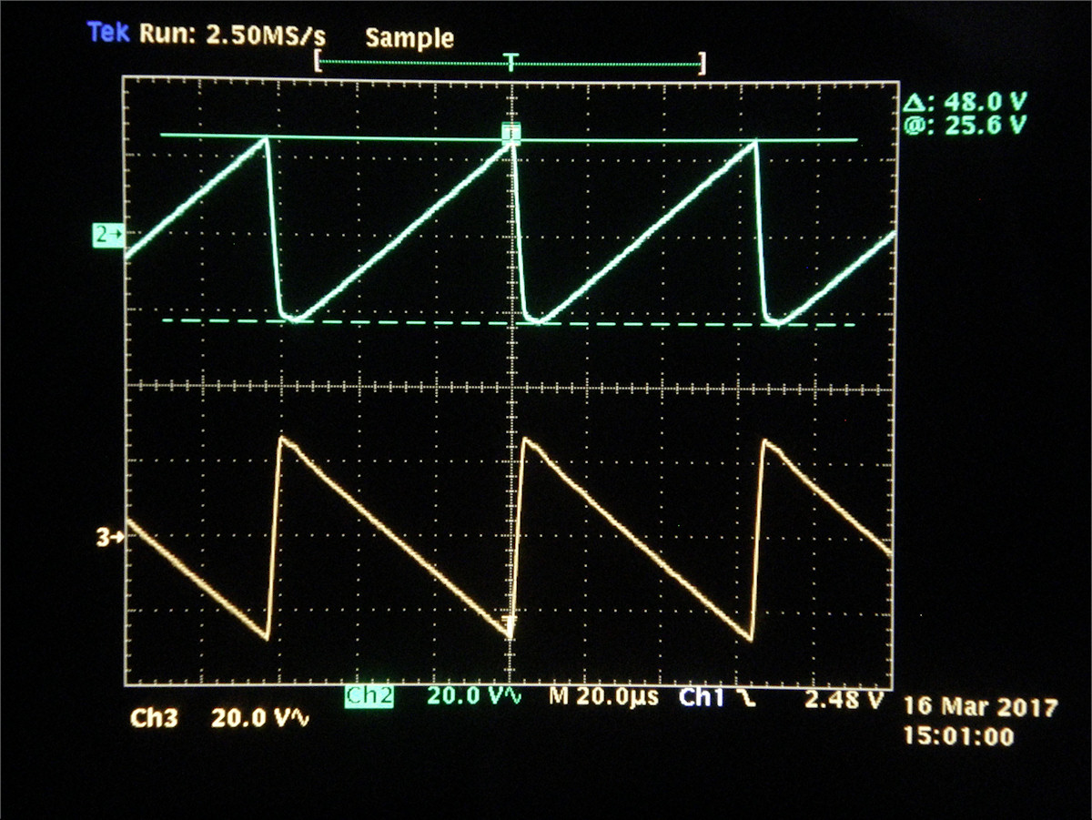
Vertical and Horizontal Deflection Circuit Waveforms - 20170316 Above we see the three major waveforms for each deflection axis. The white traces are the vertical and horizontal scan waveforms as probed at the top of the 5K SIZE pots. These run approximately zero to five volts. The oscilloscope is DC triggered on the falling edge at around 2 volts. The green and yellow traces are the AC coupled waveforms of the collectors of the high voltage amplifiers. Both waveforms are riding on just under 90 volts of DC at their midpoint. The green trace is OUT+ and the yellow is OUT-. Vertical drive to the deflection plates is 60 volts pk-pk and horizontal drive is running at about 96 volts pk-pk. 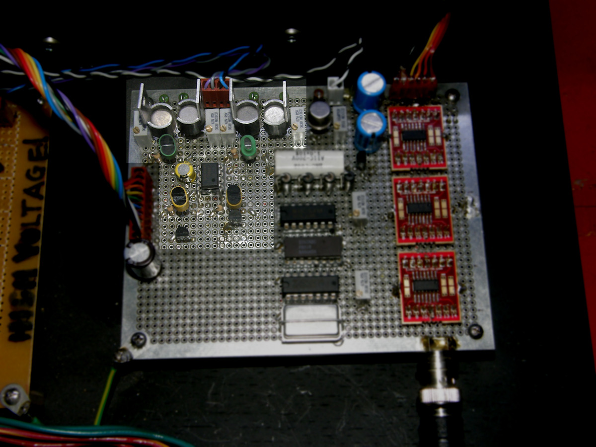
H & V Deflection Circuits Physical Construction (highlighted) The high voltage scanning amplifiers are the two pairs of transistors with heat sinks, seen in the photo above. The 100K, 1W collector load resistors are just visible behind them. The two pairs of transistors bound in green heat shrink are the negative constant current sources for the scan amps. The two pairs of transistors bound by yellow heat shrink are the positive constant current source for the ramp generators. The TL072 ramp generator dual buffer amplifier is the 8 pin DIP IC in the center. The scan reset FETS are visble just below the yellow current sources. Both scan circuits consume less than 3 square inches of board space. [HOME] [ELECTRONICS PROJECTS] [TINY IKE INDEX] [PART 5] |